Non-Destructive Measurement, Infrared and X-ray Metrology, and AI-Driven Process Optimization Drive Growth Through 2036
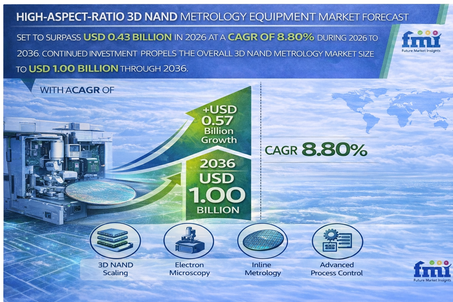
NEWARK, DE / ACCESS Newswire / March 26, 2026 / The global high-aspect-ratio 3D NAND metrology equipment market is entering a critical growth phase as memory manufacturers accelerate the transition toward ultra-high layer-count architectures exceeding 200 layers. Valued at USD 0.40 billion in 2025, the market is projected to reach USD 0.43 billion in 2026 and expand to USD 1.00 billion by 2036, registering a steady CAGR of 8.80% during the forecast period.
This growth underscores a structural transformation in semiconductor manufacturing, where traditional metrology approaches are no longer sufficient to characterize deep vertical structures. As 3D NAND architectures scale vertically, metrology systems must evolve to deliver non-destructive, high-precision measurements of subsurface features that directly impact yield and device performance.
Get Access of Report Sample:
https://www.futuremarketinsights.com/reports/sample/rep-gb-32468
Market Value Analysis: Yield Preservation and Non-Destructive Measurement Driving Demand
Between 2026 and 2030, the high-aspect-ratio 3D NAND metrology equipment market is expected to expand steadily as memory IDMs intensify investments in advanced process control systems. Procurement teams are increasingly prioritizing inline metrology platforms capable of detecting hidden defects within deep channel holes before they propagate into large-scale wafer scrap events.
Memory manufacturers are focusing on:
Non-destructive metrology solutions for deep trench and channel hole analysis
Inline measurement systems enabling real-time process feedback
Infrared and X-ray technologies for subsurface defect detection
High-throughput platforms optimized for high aspect ratio structures
Delays in upgrading metrology infrastructure force fabs to rely on destructive cross-sectioning methods, significantly increasing cycle times and reducing overall production efficiency.
From 2030 to 2036, growth will be driven by the transition toward 300-layer and beyond architectures, where conventional optical methods reach physical limitations and advanced penetrating metrology becomes indispensable.
Technology Evolution: Penetrating Metrology and AI Integration Transform Process Control
The evolution of 3D NAND metrology is being shaped by the convergence of advanced physics, material science, and data analytics. As vertical memory structures become increasingly complex, measurement technologies must balance depth penetration, resolution, and throughput.
Key innovations include:
Infrared critical dimension (IRCD) metrology for deep feature analysis
X-ray-based measurement systems for opaque multi-layer stacks
Machine learning algorithms for noise reduction and signal extraction
Advanced interferometry techniques for precise profile characterization
Hybrid metrology platforms combining optical and electron-beam methods
A key challenge lies in overcoming signal degradation as aspect ratios increase. Longer acquisition times and reduced signal-to-noise ratios require advanced computational techniques to maintain throughput without compromising accuracy.
An industry analyst notes:
"The real bottleneck in 3D NAND metrology is not just measurement capability, but throughput scalability. As layer counts increase, fabs must deploy significantly more tools to maintain sampling rates, fundamentally reshaping capital expenditure strategies."
Precision Metrology Becoming Central to 3D NAND Yield Optimization
As memory architectures scale vertically, metrology systems are emerging as mission-critical components in fabrication workflows. These systems enable:
Real-time detection of profile bowing and tilting defects
Accurate measurement of bottom critical dimensions in deep चैनnel holes
Continuous monitoring of etch process stability
Reduction in wafer scrap through early defect identification
Optimization of multi-layer alignment in stacked architectures
This shift is redefining competitive dynamics, where metrology performance directly influences yield rates, production efficiency, and cost per bit.
Segment Spotlight
IRCD Metrology Leads Technology Segment (31.0%)
Infrared-based systems dominate due to their ability to penetrate thick dielectric stacks without causing charging artifacts.
Inline Systems Dominate Deployment (58.0%)
Real-time process control drives adoption of inline metrology for continuous feedback and drift correction.
Channel Hole Measurement Leads Application (34.0%)
Deep channel structures require precise profiling to prevent catastrophic device failures.
Memory IDMs Lead End-Use Segment (49.0%)
Large-scale memory manufacturers dominate demand due to concentrated capital investments in vertical architectures.
Etch Control Leads Process Stage (37.0%)
Maintaining etch uniformity is critical for preserving structural integrity in high-aspect-ratio features.
Regional Insights: Asia-Pacific Anchors 3D NAND Metrology Expansion
The high-aspect-ratio 3D NAND metrology equipment market is highly concentrated in regions with advanced memory manufacturing ecosystems and strong semiconductor self-sufficiency initiatives.
Country |
CAGR (2026-2036) |
Key Growth Drivers |
|---|---|---|
India |
10.2% |
Government-backed semiconductor subsidies and greenfield fab investments |
China |
9.7% |
Indigenous memory scaling and self-sufficiency mandates |
South Korea |
9.3% |
Aggressive deployment of leading-edge memory technologies |
Singapore |
8.9% |
Concentrated capacity expansion by global memory players |
Japa |
8.5% |
Continuous investment in advanced memory architectures |
United States |
7.9% |
Focus on pilot lines and next-generation R&D |
Taiwan |
7.4% |
Limited memory focus compared to logic-dominated ecosystem |
Opportunities: Advanced Metrology Architectures Unlock Next-Generation Scaling
Key growth opportunities in the market include:
X-ray source miniaturization for inline deployment
Machine learning-driven signal enhancement for faster measurements
Cryogenic etch-compatible metrology systems
Hybrid platforms integrating multiple measurement modalities
Advanced process control software for predictive yield optimization
These innovations are enabling scalable, high-precision metrology solutions tailored for next-generation vertical memory manufacturing.
Competitive Landscape: Algorithmic Capability and Integration Define Leadership
The high-aspect-ratio 3D NAND metrology equipment market is characterized by a small group of highly specialized players with deep expertise in both hardware and computational metrology.
Leading companies include:
KLA Corporation
Onto Innovation
Nova Ltd.
Hitachi High-Tech Corporation
Applied Materials, Inc.
Lasertec Corporation
Camtek Ltd.
Competitive differentiation is increasingly driven by:
Ability to deliver non-destructive deep feature measurement
Integration of AI-driven data processing capabilities
Throughput optimization for high-volume manufacturing
Seamless integration with fab-wide process control systems
Future Outlook: Metrology Becomes the Backbone of Vertical Memory Scaling
Looking ahead to 2036, high-aspect-ratio metrology systems will become indispensable for enabling continued 3D NAND scaling.
Key trends include:
Transition toward fully non-destructive measurement methodologies
Increased reliance on AI-driven metrology platforms
Expansion of inline metrology across all critical process steps
Growing alignment between metrology performance and yield economics
Standardization of measurement protocols for ultra-high layer architectures
As the semiconductor industry pushes beyond 300-layer memory stacks, metrology systems will evolve from supporting tools to core enablers of scalable, high-yield manufacturing-defining the future trajectory of advanced memory technologies.
For an in-depth analysis of evolving formulation trends and to access the complete strategic outlook for the High-Aspect-Ratio 3D NAND Metrology Equipment Market through 2036, visit the official report page at: https://www.futuremarketinsights.com/reports/high-aspect-ratio-3d-nand-metrology-equipment-market
Browse More Technology Industry Reports:
Security Labels Market - https://www.futuremarketinsights.com/reports/security-labels-market
Digital Experience Platform (DXP) Market - https://www.futuremarketinsights.com/reports/digital-experience-platform-market
Accounts Payable Automation Market - https://www.futuremarketinsights.com/reports/accounts-payable-automation-market
Harmonic Filter Market - https://www.futuremarketinsights.com/reports/harmonic-filter-market
Insurtech Market - https://www.futuremarketinsights.com/reports/insurtech-market
About Future Market Insights (FMI)
Future Market Insights (FMI) is a leading provider of market intelligence and consulting services, serving clients in over 150 countries. Headquartered in Delaware, USA, with a global delivery center in India and offices in the UK and UAE, FMI delivers actionable insights to businesses across industries including automotive, technology, consumer products, manufacturing, energy, and chemicals.
An ESOMAR-certified research organization, FMI provides custom and syndicated market reports and consulting services, supporting both Fortune 1,000 companies and SMEs. Its team of 300+ experienced analysts ensures credible, data-driven insights to help clients navigate global markets and identify growth opportunities.
For Press & Corporate Inquiries
Rahul Singh
AVP - Marketing and Growth Strategy
Future Market Insights, Inc.
+91 8600020075
For Sales - sales@futuremarketinsights.com
For Media - Rahul.singh@futuremarketinsights.com
For web - https://www.futuremarketinsights.com/
SOURCE: Future Market Insights, Inc.
View the original press release on ACCESS Newswire