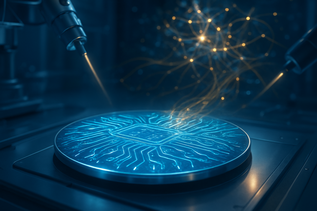
As of January 12, 2026, the global semiconductor landscape has officially entered its most transformative era in over a decade. Taiwan Semiconductor Manufacturing Company (NYSE: TSM / TPE:2330), the world’s largest contract chipmaker, has confirmed that its 2-nanometer (N2) process node is now in high-volume manufacturing (HVM). This milestone marks the end of the "FinFET" transistor era and the beginning of the "Nanosheet" era, providing the essential hardware foundation for the next generation of generative AI models, autonomous systems, and ultra-efficient mobile devices.
The shift to 2nm is more than a incremental upgrade; it is a fundamental architectural pivot designed to overcome the "power wall" that has threatened to stall AI progress. By delivering a staggering 30% reduction in power consumption compared to current 3nm technologies, TSMC is enabling a future where massive Large Language Models (LLMs) can run with significantly lower energy footprints. This announcement solidifies TSMC’s dominance in the foundry market, as the company scales production to meet the insatiable demand from the world's leading technology giants.
The Technical Leap: From Fins to Nanosheets
The core of the N2 node’s success lies in the transition from FinFET (Fin Field-Effect Transistor) to Gate-All-Around (GAA) Nanosheet transistors. For nearly 15 years, FinFET served the industry well, but as transistors shrunk toward the atomic scale, current leakage became an insurmountable hurdle. The Nanosheet design solves this by stacking horizontal layers of silicon and surrounding them on all four sides with the gate. This 360-degree control virtually eliminates leakage, allowing for tighter electrostatic management and drastically improved energy efficiency.
Technically, the N2 node offers a "full-node" leap over the previous N3E (3nm) process. According to TSMC’s engineering data, the 2nm process delivers a 10% to 15% performance boost at the same power level, or a 25% to 30% reduction in power consumption at the same clock speed. Furthermore, TSMC has introduced a proprietary technology called Nano-Flex . This allows chip designers to mix and match nanosheets of different heights within a single block—using "tall" nanosheets for high-performance compute cores and "short" nanosheets for energy-efficient background tasks. This level of granularity is unprecedented and gives designers a new toolkit for balancing the thermal and performance needs of complex AI silicon.
Initial reports from the Hsinchu and Kaohsiung fabs indicate that yield rates for the N2 node are remarkably mature, sitting between 65% and 75%. This is a significant achievement for a first-generation architectural shift, as new nodes typically struggle to reach such stability in their first few months of volume production. The integration of "Super-High-Performance Metal-Insulator-Metal" (SHPMIM) capacitors further enhances the node, providing double the capacitance density and a 50% reduction in resistance, which ensures stable power delivery for the high-frequency bursts required by AI inference engines.
The Industry Impact: Securing the AI Supply Chain
The commencement of 2nm production has sparked a gold rush among tech titans. Apple (NASDAQ: AAPL) has reportedly secured over 50% of TSMC’s initial N2 capacity through 2026. The upcoming A20 Pro chip, expected to power the next generation of iPhones and iPads, will likely be the first consumer-facing product to utilize this technology, giving Apple a significant lead in on-device "Edge AI" capabilities. Meanwhile, NVIDIA (NASDAQ: NVDA) and AMD (NASDAQ: AMD) are racing to port their next-generation AI accelerators to the N2 node. NVIDIA’s rumored "Vera Rubin" architecture and AMD’s "Venice" EPYC processors are expected to leverage the 2nm efficiency to pack more CUDA and Zen cores into the same thermal envelope.
The competitive landscape is also shifting. While Samsung (KRX:005930) was technically the first to move to GAA at the 3nm stage, it has struggled with yield issues, leading many major customers to remain with TSMC for the 2nm transition. Intel (NASDAQ: INTC) remains the most aggressive challenger with its 18A node, which includes "PowerVia" (back-side power delivery) ahead of TSMC’s roadmap. However, industry analysts suggest that TSMC’s manufacturing scale and "yield learning curve" give it a massive commercial advantage. Hyperscalers like Amazon (NASDAQ: AMZN), Alphabet/Google (NASDAQ: GOOGL), and Microsoft (NASDAQ: MSFT) are also lining up for N2 capacity to build custom AI ASICs, aiming to reduce their reliance on off-the-shelf hardware and lower the massive electricity bills associated with their data centers.
The Broader Significance: Breaking the Power Wall
The arrival of 2nm silicon comes at a critical juncture for the AI industry. As LLMs move toward tens of trillions of parameters, the environmental and economic costs of training and running these models have become a primary concern. The 30% power reduction offered by N2 acts as a "pressure release valve" for the global energy grid. By allowing for more "tokens per watt," the 2nm node enables the scaling of generative AI without a linear increase in carbon emissions or infrastructure costs.
Furthermore, this development accelerates the rise of "Physical AI" and robotics. For an autonomous robot or a self-driving car to process complex visual data in real-time, it requires massive compute power within a limited battery and thermal budget. The efficiency of Nanosheet transistors makes these applications more viable, moving AI from the cloud to the physical world. However, the transition is not without its hurdles. The cost of 2nm wafers is estimated to be between $25,000 and $30,000, a 50% increase over 3nm. This "silicon inflation" may widen the gap between the tech giants who can afford the latest nodes and smaller startups that may be forced to rely on older, less efficient hardware.
Future Horizons: The Path to 1nm and Beyond
TSMC’s roadmap does not stop at N2. The company has already outlined plans for N2P, an enhanced version of the 2nm node, followed by the A16 (1.6nm) node in late 2026. The A16 node will be the first to feature "Super Power Rail," TSMC’s version of back-side power delivery, which moves power wiring to the underside of the wafer to free up more space for signal routing. Beyond that, the A14 (1.4nm) and A10 (1nm) nodes are already in the research and development phase, with the latter expected to explore new materials like 2D semiconductors to replace traditional silicon.
One of the most watched developments will be TSMC’s adoption of High-NA EUV lithography machines from ASML (NASDAQ: ASML). While Intel has already begun using these $380 million machines, TSMC is taking a more conservative approach, opting to stick with existing Low-NA EUV for the initial N2 ramp-up to keep costs manageable and yields high. This strategic divergence between the two semiconductor giants will likely determine the leadership of the foundry market for the remainder of the decade.
A New Chapter in Computing History
The official start of volume production for TSMC’s 2nm process is a watershed moment in computing history. It represents the successful navigation of one of the most difficult engineering transitions the industry has ever faced. By mastering the Nanosheet architecture, TSMC has ensured that Moore’s Law—or at least its spirit—continues to drive the AI revolution forward. The immediate significance lies in the massive efficiency gains that will soon be felt in everything from flagship smartphones to the world’s most powerful supercomputers.
In the coming months, the industry will be watching closely for the first third-party benchmarks of 2nm silicon. As the first chips roll off the assembly lines in Taiwan and head to packaging facilities, the true impact of the Nanosheet era will begin to materialize. For now, TSMC has once again proven that it is the indispensable linchpin of the global technology ecosystem, providing the literal foundation upon which the future of artificial intelligence is being built.
This content is intended for informational purposes only and represents analysis of current AI developments.
TokenRing AI delivers enterprise-grade solutions for multi-agent AI workflow orchestration, AI-powered development tools, and seamless remote collaboration platforms.
For more information, visit https://www.tokenring.ai/.