As of January 13, 2026, the global race for artificial intelligence supremacy has moved beyond the simple shrinking of transistors. The industry has entered the era of the "Packaging Fortress," where the ability to stitch multiple silicon dies together is now more valuable than the silicon itself. Taiwan Semiconductor Manufacturing Co. (TPE:2330) (NYSE: TSM) has responded to this shift by signaling a massive surge in capital expenditure, projected to reach between $44 billion and $50 billion for the 2026 fiscal year. This unprecedented investment is aimed squarely at expanding advanced packaging capacity—specifically CoWoS (Chip on Wafer on Substrate) and SoIC (System on Integrated Chips)—to satisfy the voracious appetite of the world’s AI giants.
Despite massive expansions throughout 2025, the demand for high-end AI accelerators remains "over-subscribed." The recent launch of the NVIDIA (NASDAQ: NVDA) Rubin architecture and the upcoming AMD (NASDAQ: AMD) Instinct MI400 series has created a structural bottleneck that is no longer about raw wafer starts, but about the complex "back-end" assembly required to integrate high-bandwidth memory (HBM4) and multiple compute chiplets into a single, massive system-in-package.
The Technical Frontier: CoWoS-L and the 3D Stacking Revolution
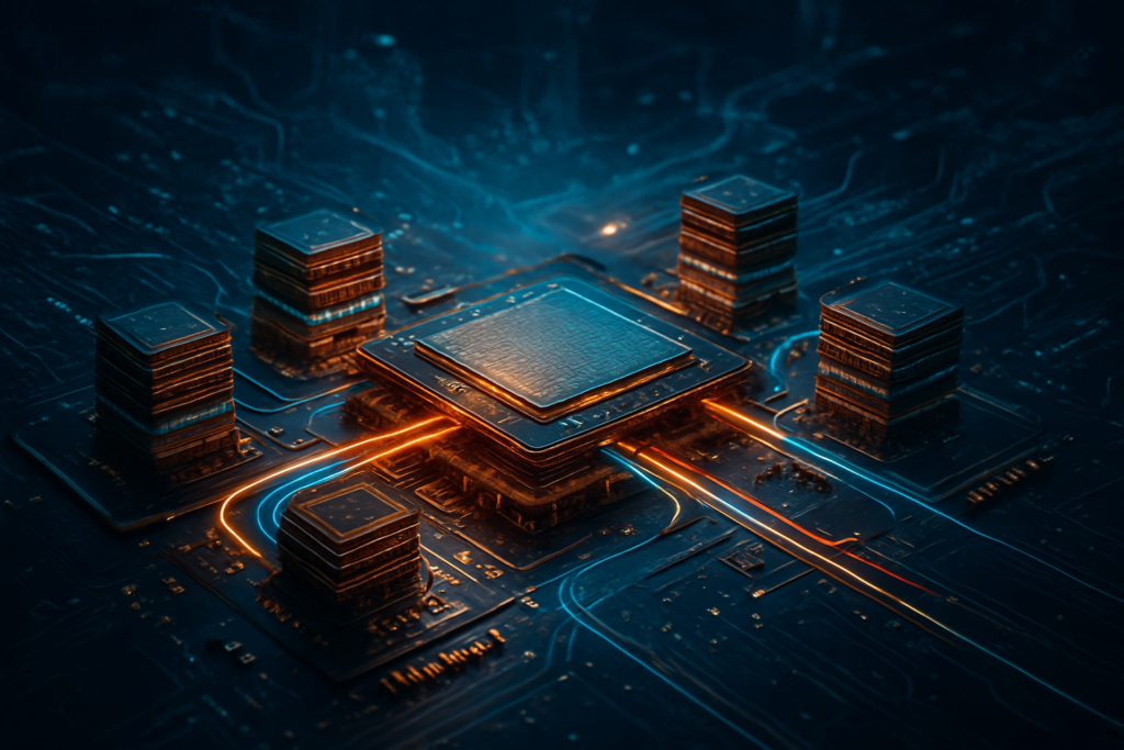
The technical specifications of 2026’s flagship AI chips have pushed traditional manufacturing to its physical limits. For years, the "reticle limit"—the maximum size of a single chip that a lithography machine can print—stood at roughly 858 mm². To bypass this, TSMC has pioneered CoWoS-L (Local Silicon Interconnect), which uses tiny silicon "bridges" to link multiple chiplets across a larger substrate. This allows NVIDIA’s Rubin chips to function as a single logical unit while physically spanning an area equivalent to three or four traditional processors.
Furthermore, 3D stacking via SoIC-X (System on Integrated Chips) has transitioned from an experimental boutique process to a mainstream requirement. Unlike 2.5D packaging, which places chips side-by-side, SoIC stacks them vertically using "bumpless" copper-to-copper hybrid bonding. By early 2026, commercial bond pitches have reached a staggering 6 micrometers. This technical leap reduces signal latency by 40% and cuts interconnect power consumption by half, a critical factor for data centers struggling with the 1,000-watt power envelopes of modern AI "superchips."
The integration of HBM4 memory marks the third pillar of this technical shift. As the interface width for HBM4 has doubled to 2048-bit, the complexity of aligning these memory stacks on the interposer has become a primary engineering challenge. Industry experts note that while TSMC has increased its CoWoS capacity to over 120,000 wafers per month, the actual yield of finished systems is currently constrained by the precision required to bond these high-density memory stacks without defects.
The Allocation War: NVIDIA and AMD’s Battle for Capacity
The business implications of the packaging bottleneck are stark: if you don’t own the packaging capacity, you don’t own the market. NVIDIA has aggressively moved to secure its dominance, reportedly pre-booking 60% to 65% of TSMC’s total CoWoS output for 2026. This "capacity moat" ensures that the Rubin series—which integrates up to 12 stacks of HBM4—can be produced at a scale that competitors struggle to match. This strategic lock-in has forced other players to fight for the remaining 35% of the world's most advanced assembly lines.
AMD has emerged as the most formidable challenger, securing approximately 11% of TSMC’s 2026 capacity for its Instinct MI400 series. Unlike previous generations, AMD is betting heavily on SoIC 3D stacking to gain a density advantage over NVIDIA. By stacking cache and compute logic vertically, AMD aims to offer superior performance-per-watt, targeting hyperscale cloud providers who are increasingly sensitive to the total cost of ownership (TCO) and electricity consumption of their AI clusters.
This concentration of power at TSMC has sparked a strategic pivot among other tech giants. Apple (NASDAQ: AAPL) has reportedly secured significant SoIC capacity for its next-generation "M5 Ultra" chips, signaling that advanced packaging is no longer just for data center GPUs but is moving into high-end consumer silicon. Meanwhile, Intel (NASDAQ: INTC) and Samsung (KRX:005930) are racing to offer "turnkey" alternatives, though they continue to face uphill battles in matching TSMC’s yield rates and ecosystem integration.
A Fundamental Shift in the Moore’s Law Paradigm
The 2026 packaging crunch represents a wider historical significance: the functional end of traditional Moore’s Law scaling. For five decades, the industry relied on making transistors smaller to gain performance. Today, that "node shrink" is so expensive and yields such diminishing returns that the industry has shifted its focus to "System Technology Co-Optimization" (STCO). In this new landscape, the way chips are connected is just as important as the 3nm or 2nm process used to print them.
This shift has profound geopolitical and economic implications. The "Silicon Shield" of Taiwan has been reinforced not just by the ability to make chips, but by the concentration of advanced packaging facilities like TSMC’s new AP7 and AP8 plants. The announcement of the first US-based advanced packaging plant (AP1) in Arizona, scheduled to begin construction in early 2026, highlights the desperate push by the U.S. government to bring this critical "back-end" infrastructure onto American soil to ensure supply chain resilience.
However, the transition to chiplets and 3D stacking also brings new concerns. The complexity of these systems makes them harder to repair and more prone to "silent data errors" if the interconnects degrade over time. Furthermore, the high cost of advanced packaging is creating a "digital divide" in the hardware space, where only the wealthiest companies can afford to build or buy the most advanced AI hardware, potentially centralizing AI power in the hands of a few trillion-dollar entities.
Future Outlook: Glass Substrates and Optical Interconnects
Looking ahead to the latter half of 2026 and into 2027, the industry is already preparing for the next evolution in packaging: glass substrates. While current organic substrates are reaching their limits in terms of flatness and heat resistance, glass offers the structural integrity needed for even larger "system-on-wafer" designs. TSMC, Intel, and Samsung are all in a high-stakes R&D race to commercialize glass substrates, which could allow for even denser interconnects and better thermal management.
We are also seeing the early stages of "Silicon Photonics" integration directly into the package. Near-term developments suggest that by 2027, optical interconnects will replace traditional copper wiring for chip-to-chip communication, effectively moving data at the speed of light within the server rack. This would solve the "memory wall" once and for all, allowing thousands of chiplets to act as a single, unified brain.
The primary challenge remains yield and cost. As packaging becomes more complex, the risk of a single faulty chiplet ruining a $40,000 "superchip" increases. Experts predict that the next two years will see a massive surge in AI-driven inspection and metrology tools, where AI is used to monitor the manufacturing of the very hardware that runs it, creating a self-reinforcing loop of technological advancement.
Conclusion: The New Era of Silicon Integration
The advanced packaging bottleneck of 2026 is a defining moment in the history of computing. It marks the transition from the era of the "monolithic chip" to the era of the "integrated system." TSMC’s massive $50 billion CapEx surge is a testament to the fact that the future of AI is being built in the packaging house, not just the foundry. With NVIDIA and AMD locked in a high-stakes battle for capacity, the ability to master 3D stacking and CoWoS-L has become the ultimate competitive advantage.
As we move through 2026, the industry's success will depend on its ability to solve the HBM4 yield issues and successfully scale new facilities in Taiwan and abroad. The "Packaging Fortress" is now the most critical infrastructure in the global economy. Investors and tech leaders should watch closely for quarterly updates on TSMC’s packaging yields and the progress of the Arizona AP1 facility, as these will be the true bellwethers for the next phase of the AI revolution.
This content is intended for informational purposes only and represents analysis of current AI developments.
TokenRing AI delivers enterprise-grade solutions for multi-agent AI workflow orchestration, AI-powered development tools, and seamless remote collaboration platforms.
For more information, visit https://www.tokenring.ai/.


