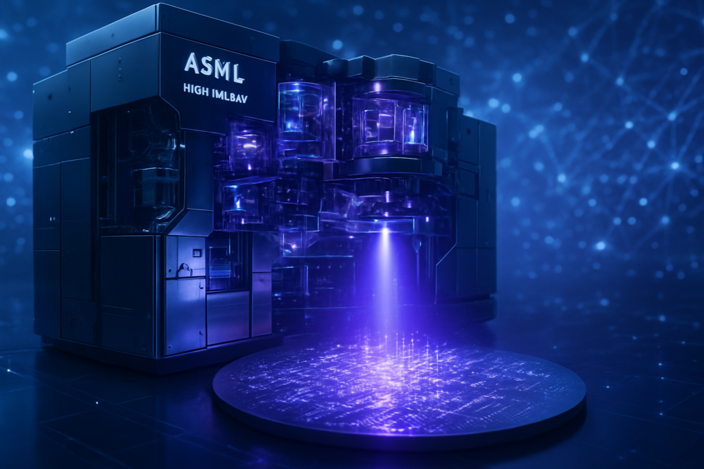
As of January 5, 2026, the semiconductor industry has officially entered the "Angstrom Era," a transition marked by the high-volume deployment of the most complex machine ever built: the High-Numerical Aperture (High-NA) Extreme Ultraviolet (EUV) lithography scanner. Developed by ASML (NASDAQ: ASML), the Twinscan EXE:5200B has become the defining tool for the sub-2nm generation of chips. This technological leap is not merely an incremental upgrade; it is the gatekeeper for the next decade of Moore’s Law, providing the precision necessary to print transistors at scales where atoms are the primary unit of measurement.
The immediate significance of this development lies in the radical shift of the competitive landscape. Intel (NASDAQ: INTC), after a decade of trailing its rivals, has seized the "first-mover" advantage by becoming the first to integrate High-NA into its production lines. This aggressive stance is aimed directly at reclaiming the process leadership crown from TSMC (NYSE: TSM), which has opted for a more conservative, cost-optimized approach. As AI workloads demand exponentially more compute density and power efficiency, the success of High-NA EUV will dictate which silicon giants will power the next generation of generative AI models and hyperscale data centers.
The Twinscan EXE:5200B: Engineering the Sub-2nm Frontier
The technical specifications of the Twinscan EXE:5200B represent a paradigm shift in lithography. The "High-NA" designation refers to the increase in numerical aperture from 0.33 in standard EUV machines to 0.55. This change allows the machine to achieve a staggering 8nm resolution, enabling the printing of features approximately 1.7 times smaller than previous tools. In practical terms, this translates to a 2.9x increase in transistor density, allowing engineers to cram billions more gates onto a single piece of silicon without the need for the complex "multi-patterning" techniques that have plagued 3nm and 2nm yields.
Beyond resolution, the EXE:5200B addresses the two most significant hurdles of early High-NA prototypes: throughput and alignment. The production-ready model now achieves a throughput of 175 to 200 wafers per hour (wph), matching the productivity of the latest low-NA scanners. Furthermore, it boasts an overlay accuracy of 0.7nm. This sub-nanometer precision is critical for a process known as "field stitching." Because High-NA optics halve the exposure field size, larger chips—such as the massive GPUs produced by NVIDIA (NASDAQ: NVDA)—must be printed in two separate halves. The 0.7nm overlay ensures these halves are aligned with such perfection that they function as a single, seamless monolithic die.
This approach differs fundamentally from the industry's previous trajectory. For the past five years, foundries have relied on "multi-patterning," where a single layer is printed using multiple exposures to achieve finer detail. While effective, multi-patterning increases the risk of defects and significantly lengthens the manufacturing cycle. High-NA EUV returns the industry to "single-patterning" for the most critical layers, drastically simplifying the manufacturing flow and improving the "time-to-market" for cutting-edge designs. Initial reactions from the research community suggest that while the $380 million price tag per machine is daunting, the reduction in process steps and the jump in density make it an inevitable necessity for the sub-2nm era.
A Tale of Two Strategies: Intel’s Leap vs. TSMC’s Caution
The deployment of High-NA EUV has created a strategic schism between the world’s leading chipmakers. Intel has positioned itself as the "High-NA Vanguard," utilizing the EXE:5200B to underpin its 18A (1.8nm) and 14A (1.4nm) nodes. By early 2026, Intel's 18A process has reached high-volume manufacturing, with the first "Panther Lake" consumer chips hitting shelves. While 18A was designed to be compatible with standard EUV, Intel is selectively using High-NA tools to "de-risk" the technology before its 14A node becomes "High-NA native" later this year. This early adoption is a calculated risk to prove to foundry customers that Intel Foundry is once again the world's most advanced manufacturer.
Conversely, TSMC has maintained a "wait-and-see" approach, focusing on optimizing its existing low-NA EUV infrastructure for its A14 (1.4nm) node. TSMC’s leadership has argued that the current cost-per-wafer for High-NA is too high for mass-market mobile chips, preferring to use multi-patterning on its ultra-mature NXE:3800E scanners. This creates a fascinating market dynamic: Intel is betting on technical superiority and process simplification to attract high-margin AI customers, while TSMC is betting on cost-efficiency and yield stability.
The implications for the broader market are profound. If Intel successfully scales 14A using the EXE:5200B, it could potentially offer AI companies like AMD (NASDAQ: AMD) and even NVIDIA a performance-per-watt advantage that TSMC cannot match until its own High-NA transition, currently slated for 2027 or 2028. This disruption could shift the balance of power in the foundry business, which TSMC has dominated for over a decade. Startups specializing in "AI-first" silicon also stand to benefit, as the single-patterning capability of High-NA reduces the "design-to-chip" lead time, allowing for faster iteration of specialized neural processing units (NPUs).
The Silicon Gatekeeper of the AI Revolution
The significance of ASML’s High-NA dominance extends far beyond corporate rivalry; it is the physical foundation of the AI revolution. Modern Large Language Models (LLMs) are currently constrained by two factors: the amount of high-speed memory that can be placed near the compute units and the power efficiency of the data center. Sub-2nm chips produced with the EXE:5200B are expected to consume 25% to 35% less power for the same frequency compared to 3nm equivalents. In an era where electricity and cooling costs are the primary bottlenecks for AI scaling, these efficiency gains are worth billions to hyperscalers like Microsoft (NASDAQ: MSFT) and Google (NASDAQ: GOOGL).
Furthermore, the transition to High-NA mirrors previous industry milestones, such as the initial shift from DUV to EUV in 2019. Just as that transition enabled the 5nm and 3nm chips that power today’s smartphones and AI accelerators, High-NA is the "second act" of EUV that will carry the industry toward the 1nm mark. However, the stakes are higher now. The geopolitical importance of semiconductor leadership has never been greater, and the "High-NA club" is currently an exclusive group. With ASML being the sole provider of these machines, the global supply chain for the most advanced AI hardware now runs through a single point of failure in Veldhoven, Netherlands.
Potential concerns remain regarding the "halved field" issue. While field stitching has been proven in the lab, doing it at a scale of millions of units per month without impacting yield is a monumental challenge. If the stitching process leads to higher defect rates, the cost of the world’s most advanced AI GPUs could skyrocket, potentially slowing the democratization of AI compute. Nevertheless, the industry has historically overcome such lithographic hurdles, and the consensus is that High-NA is the only viable path forward.
The Road to 14A and Beyond
Looking ahead, the next 24 months will be critical for the validation of High-NA technology. Intel is expected to release its 14A Process Design Kit (PDK 1.0) to foundry customers in the coming months, which will be the first design environment built entirely around the capabilities of the EXE:5200B. This node will introduce "PowerDirect," a second-generation backside power delivery system that, when combined with High-NA lithography, promises a 20% performance boost over the already impressive 18A node.
Experts predict that by 2028, the "High-NA gap" between Intel and TSMC will close as the latter finally integrates the tools into its "A14P" process. However, the "learning curve" advantage Intel is building today could prove difficult to overcome. We are also likely to see the emergence of "Hyper-NA" research—tools with numerical apertures even higher than 0.55—as the industry begins to look toward the sub-10-angstrom (sub-1nm) era in the 2030s. The immediate challenge for ASML and its partners will be to drive down the cost of these machines and improve the longevity of the specialized photoresists and masks required for such extreme resolutions.
A New Chapter in Computing History
The deployment of the ASML Twinscan EXE:5200B marks a definitive turning point in the history of computing. By enabling the mass production of sub-2nm chips, ASML has effectively extended the life of Moore’s Law at a time when many predicted its demise. Intel’s aggressive adoption of this technology represents a "moonshot" attempt to regain its former glory, while the industry’s shift toward "Angstrom-class" silicon provides the necessary hardware runway for the next decade of AI innovation.
The key takeaways are clear: the EXE:5200B is the most productive and precise lithography tool ever created, Intel is currently the only player using it for high-volume manufacturing, and the future of AI hardware is now inextricably linked to the success of High-NA EUV. In the coming weeks and months, all eyes will be on Intel’s 18A yield reports and the first customer tape-outs for the 14A node. These metrics will serve as the first real-world evidence of whether the High-NA era will deliver on its promise of a new golden age for silicon.
This content is intended for informational purposes only and represents analysis of current AI developments.
TokenRing AI delivers enterprise-grade solutions for multi-agent AI workflow orchestration, AI-powered development tools, and seamless remote collaboration platforms.
For more information, visit https://www.tokenring.ai/.