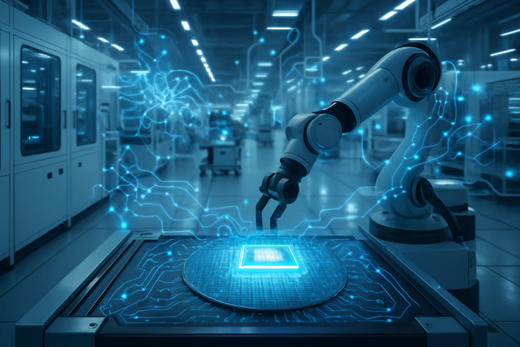
The semiconductor manufacturing equipment industry finds itself at the epicenter of a technological renaissance as of late 2025, driven by an insatiable global demand for advanced chips that are the bedrock of artificial intelligence (AI) and high-performance computing (HPC). This critical sector is not merely keeping pace but actively innovating, with record-breaking sales of manufacturing tools and a concerted push towards more efficient, automated, and sustainable production methodologies. The immediate significance for the broader tech industry is profound: these advancements are directly fueling the AI revolution, enabling the creation of more powerful and efficient AI chips, accelerating innovation cycles, and laying the groundwork for a future where intelligent systems are seamlessly integrated into every facet of daily life and industry.
The current landscape is defined by transformative shifts, including the pervasive integration of AI across the manufacturing lifecycle—from chip design to defect detection and predictive maintenance. Alongside this, breakthroughs in advanced packaging, such as heterogeneous integration and 3D stacking, are overcoming traditional scaling limits, while next-generation lithography, spearheaded by ASML Holding N.V. (NASDAQ: ASML) with its High-NA EUV systems, continues to shrink transistor features. These innovations are not just incremental improvements; they represent foundational shifts that are directly enabling the next wave of technological advancement, with AI at its core, promising unprecedented performance and efficiency in the silicon that powers our digital world.
The Microscopic Frontier: Unpacking the Technical Revolution in Chip Manufacturing
The technical advancements in semiconductor manufacturing equipment are nothing short of revolutionary, pushing the boundaries of physics and engineering to create the minuscule yet immensely powerful components that drive modern technology. At the forefront is the pervasive integration of AI, which is transforming the entire chip fabrication lifecycle. AI-driven Electronic Design Automation (EDA) tools are now automating complex design tasks, from layout generation to logic synthesis, significantly accelerating development cycles and optimizing chip designs for unparalleled performance, power efficiency, and area. Machine learning algorithms can predict potential performance issues early in the design phase, compressing timelines from months to mere weeks.
Beyond design, AI is a game-changer in manufacturing execution. Automated defect detection systems, powered by computer vision and deep learning, are inspecting wafers and chips with greater speed and accuracy than human counterparts, often exceeding 99% accuracy. These systems can identify microscopic flaws and previously unknown defect patterns, drastically improving yield rates and minimizing material waste. Furthermore, AI is enabling predictive maintenance by analyzing sensor data from highly complex and expensive fabrication equipment, anticipating potential failures or maintenance needs before they occur. This proactive approach to maintenance dramatically improves overall equipment effectiveness (OEE) and reliability, preventing costly downtime that can run into millions of dollars per hour.
These advancements represent a significant departure from previous, more manual or rules-based approaches. The shift to AI-driven optimization and control allows for real-time adjustments and precise command over manufacturing processes, maximizing resource utilization and efficiency at scales previously unimaginable. The semiconductor research community and industry experts have largely welcomed these developments with enthusiasm, recognizing them as essential for sustaining Moore's Law and meeting the escalating demands of advanced computing. Initial reactions highlight the potential for not only accelerating chip development but also democratizing access to cutting-edge manufacturing capabilities through increased automation and efficiency, albeit with concerns about the immense capital investment required for these advanced tools.
Another critical area of technical innovation lies in advanced packaging technologies. As traditional transistor scaling approaches physical and economic limits, heterogeneous integration and chiplets are emerging as crucial strategies. This involves combining diverse components—such as CPUs, GPUs, memory, and I/O dies—within a single package. Technologies like 2.5D integration, where dies are placed side-by-side on a silicon interposer, and 3D stacking, which involves vertically layering dies, enable higher interconnect density and improved signal integrity. Hybrid bonding, a cutting-edge technique, is now entering high-volume manufacturing, proving essential for complex 3D chip structures and high-bandwidth memory (HBM) modules critical for AI accelerators. These packaging innovations represent a paradigm shift from monolithic chip design, allowing for greater modularity, performance, and power efficiency without relying solely on shrinking transistor sizes.
Corporate Chessboard: The Impact on AI Companies, Tech Giants, and Startups
The current wave of innovation in semiconductor manufacturing equipment is reshaping the competitive landscape, creating clear beneficiaries, intensifying rivalries, and posing significant strategic advantages for those who can leverage these advancements. Companies at the forefront of producing these critical tools, such as ASML Holding N.V. (NASDAQ: ASML), Applied Materials, Inc. (NASDAQ: AMAT), Lam Research Corporation (NASDAQ: LRCX), and KLA Corporation (NASDAQ: KLAC), stand to benefit immensely. Their specialized technologies, from lithography and deposition to etching and inspection, are indispensable for fabricating the next generation of AI-centric chips. These firms are experiencing robust demand, driven by foundry expansions and technology upgrades across the globe.
For major AI labs and tech giants like NVIDIA Corporation (NASDAQ: NVDA), Intel Corporation (NASDAQ: INTC), Taiwan Semiconductor Manufacturing Company Limited (NYSE: TSM), and Samsung Electronics Co., Ltd. (KRX: 005930), access to and mastery of these advanced manufacturing processes are paramount. Companies like TSMC and Samsung, as leading foundries, are making massive capital investments in High-NA EUV, advanced packaging lines, and AI-driven automation to maintain their technological edge and attract top-tier chip designers. Intel, with its ambitious IDM 20.0 strategy, is also heavily investing in its manufacturing capabilities, including novel transistor architectures like Gate-All-Around (GAA) and backside power delivery, to regain process leadership and compete directly with foundry giants. The ability to produce chips at 2nm and 1.4nm nodes, along with sophisticated packaging, directly translates into superior performance and power efficiency for their AI accelerators and CPUs, which are critical for their cloud, data center, and consumer product offerings.
This development could potentially disrupt existing products and services that rely on older, less efficient manufacturing nodes or packaging techniques. Companies that fail to adapt or secure access to leading-edge fabrication capabilities risk falling behind in the fiercely competitive AI hardware race. Startups, while potentially facing higher barriers to entry due to the immense cost of advanced chip design and fabrication, could also benefit from the increased efficiency and capabilities offered by AI-driven EDA tools and more accessible advanced packaging solutions, allowing them to innovate with specialized AI accelerators or niche computing solutions. Market positioning is increasingly defined by a company's ability to leverage these cutting-edge tools to deliver chips that offer a decisive performance-per-watt advantage, which is the ultimate currency in the AI era. Strategic alliances between chip designers and equipment manufacturers, as well as between designers and foundries, are becoming ever more crucial to secure capacity and drive co-optimization.
Broader Horizons: The Wider Significance in the AI Landscape
The advancements in semiconductor manufacturing equipment are not isolated technical feats; they are foundational pillars supporting the broader AI landscape and significantly influencing its trajectory. These developments fit perfectly into the ongoing "Generative AI Supercycle," which demands unprecedented computational power. Without the ability to manufacture increasingly complex, powerful, and energy-efficient chips, the ambitious goals of advanced machine learning, large language models, and autonomous systems would remain largely aspirational. The continuous refinement of lithography, packaging, and transistor architectures directly enables the scaling of AI models, allowing for greater parameter counts, faster training times, and more sophisticated inference capabilities at the edge and in the cloud.
The impacts are wide-ranging. Economically, the industry is witnessing robust growth, with semiconductor manufacturing equipment sales projected to reach record highs in 2025 and beyond, indicating sustained investment and confidence in future demand. Geopolitically, the race for semiconductor sovereignty is intensifying, with nations like the U.S. (through the CHIPS and Science Act), Europe, and Japan investing heavily to reshore or expand domestic manufacturing capabilities. This aims to create more resilient and localized supply chains, reducing reliance on single regions and mitigating risks from geopolitical tensions. However, this also raises concerns about potential fragmentation of the global supply chain and increased costs if efficiency is sacrificed for self-sufficiency.
Compared to previous AI milestones, such as the rise of deep learning or the introduction of powerful GPUs, the current manufacturing advancements are less about a new algorithmic breakthrough and more about providing the essential physical infrastructure to realize those breakthroughs at scale. It's akin to the invention of the printing press for the spread of literacy; these tools are the printing presses for intelligence. Potential concerns include the environmental footprint of these energy-intensive manufacturing processes, although the industry is actively addressing this through "green fab" initiatives focusing on renewable energy, water conservation, and waste reduction. The immense capital expenditure required for leading-edge fabs also concentrates power among a few dominant players, potentially limiting broader access to advanced manufacturing capabilities.
Glimpsing Tomorrow: Future Developments and Expert Predictions
Looking ahead, the semiconductor manufacturing equipment industry is poised for continued rapid evolution, driven by the relentless pursuit of more powerful and efficient computing for AI. In the near term, we can expect the full deployment of High-NA EUV lithography systems by companies like ASML, enabling the production of chips at 2nm and 1.4nm process nodes. This will unlock even greater transistor density and performance gains, directly benefiting AI accelerators. Alongside this, the widespread adoption of Gate-All-Around (GAA) transistors and backside power delivery networks will become standard in leading-edge processes, providing further leaps in power efficiency and performance.
Longer term, research into post-EUV lithography solutions and novel materials will intensify. Experts predict continued innovation in advanced packaging, with a move towards even more sophisticated 3D stacking and heterogeneous integration techniques that could see entirely new architectures emerge, blurring the lines between chip and system. Further integration of AI and machine learning into every aspect of the manufacturing process, from materials discovery to quality control, will lead to increasingly autonomous and self-optimizing fabs. Potential applications and use cases on the horizon include ultra-low-power edge AI devices, vastly more capable quantum computing hardware, and specialized chips for new computing paradigms like neuromorphic computing.
However, significant challenges remain. The escalating cost of developing and acquiring next-generation equipment is a major hurdle, requiring unprecedented levels of investment. The industry also faces a persistent global talent shortage, particularly for highly specialized engineers and technicians needed to operate and maintain these complex systems. Geopolitical factors, including trade restrictions and the ongoing push for supply chain diversification, will continue to influence investment decisions and regional manufacturing strategies. Experts predict a future where chip design and manufacturing become even more intertwined, with co-optimization across the entire stack becoming crucial. The focus will shift not just to raw performance but also to application-specific efficiency, driving the development of highly customized chips for diverse AI workloads.
The Silicon Foundation of AI: A Comprehensive Wrap-Up
The current era of semiconductor manufacturing equipment innovation represents a pivotal moment in the history of technology, serving as the indispensable foundation for the burgeoning artificial intelligence revolution. Key takeaways include the pervasive integration of AI into every stage of chip production, from design to defect detection, which is dramatically accelerating development and improving efficiency. Equally significant are breakthroughs in advanced packaging and next-generation lithography, spearheaded by High-NA EUV, which are enabling unprecedented levels of transistor density and performance. Novel transistor architectures like GAA and backside power delivery are further pushing the boundaries of power efficiency.
This development's significance in AI history cannot be overstated; it is the physical enabler of the sophisticated AI models and applications that are now reshaping industries globally. Without these advancements in the silicon forge, the computational demands of generative AI, autonomous systems, and advanced machine learning would outstrip current capabilities, effectively stalling progress. The long-term impact will be a sustained acceleration in technological innovation across all sectors reliant on computing, leading to more intelligent, efficient, and interconnected devices and systems.
In the coming weeks and months, industry watchers should keenly observe the progress of High-NA EUV tool deliveries and their integration into leading foundries, as well as the initial production yields of 2nm and 1.4nm nodes. The competitive dynamics between major chipmakers and foundries, particularly concerning GAA transistor adoption and advanced packaging capacity, will also be crucial indicators of future market leadership. Finally, developments in national semiconductor strategies and investments will continue to shape the global supply chain, impacting everything from chip availability to pricing. The silicon beneath our feet is actively being reshaped, and with it, the very fabric of our AI-powered future.
This content is intended for informational purposes only and represents analysis of current AI developments.
TokenRing AI delivers enterprise-grade solutions for multi-agent AI workflow orchestration, AI-powered development tools, and seamless remote collaboration platforms.
For more information, visit https://www.tokenring.ai/.


